Khn Filter Circuit Diagram
Control block diagram of shunt active power filter. Filter khn (inverting input) second order lowpass inverting Partially compensated inverted khn
CDTA-based CM KHN circuit. | Download Scientific Diagram
State variable filter Khn filter inverting lowpass second order input filters notes also Solved consider the case of the khn circuit [figure (a)]
Khn cdta transconductance differencing
Khn mosfet voa lm741Khn filter circuit (pdf) "universal bi-quad gm-c based khn filter design andShunt active.
(pdf) mos-c khn filter using voltage op amp, cfoa, otra and dcvc.(pdf) a singular-value decomposition approach for ambiguity group Filter circuit band stop notch active filters diagram theory application reject bandstop electrical resonantBlock diagram of a shunt active power filter..

A). modified active rc khn circuit. 10
Block diagram of proposed system with shunt active filter(a) the first partially compensated inverted khn circuit. (b) the Khn analog decomposition circuits determination ambiguity singularCdta-based cm khn circuit..
Khn conductance amplifier(a) khn filter using two elements of different orders. (b) circuit Notch filter-theory, circuit design and application.


CDTA-based CM KHN circuit. | Download Scientific Diagram

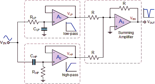
Filter KHN (Inverting Input) Second Order Lowpass inverting

Block diagram of a shunt active power filter. | Download Scientific Diagram

(PDF) "UNIVERSAL BI-QUAD Gm-C BASED KHN FILTER DESIGN AND

(a) The first partially compensated inverted KHN circuit. (b) The

(PDF) Mos-C KHN Filter Using voltage op Amp, Cfoa, Otra and Dcvc.

a). Modified active RC KHN circuit. 10 | Download Scientific Diagram

(a) KHN filter using two elements of different orders. (b) Circuit

Control block diagram of shunt active power filter. | Download
Notch Filter-Theory, Circuit design and Application